Microscopic 3D-Printed Gold Walls Could Make More Sensitive Touchscreens
By GCRU Gold News on Saturday, January 9 2016, 01:30 - Permalink
Touchscreens use a mesh of almost-transparent electronics to detect where they’re being touched. Now, a new microscopic 3D printing technique could provide greater transparency and higher sensitivity than the existing state-of-the-art.
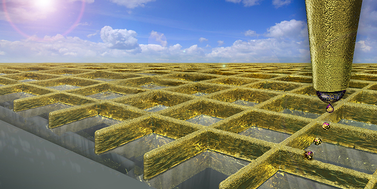
Researchers from the Swiss Federal Institute of Technology in Zurich have developed a new way to create a gird of ultra-fine conductors that could replace part of the circuitry used in today’s touchscreens. The technique, called Nanodrip, uses ink-jet printing to deposit electrohydrodynamic ink in the form of grid, gradually building up ‘nanowalls’ that act as conductors.
The ink that’s used is made up of gold nanoparticles held in a solvent. As the ink is deposited, the solvent evaporates, allowing a solid structure to be built. The result is a criss-crossing grid of gold walls, whose thickness can vary between 80 and 500 nanometers. Crucially, the walls are up to four times taller than they are wide, which means their cross-section is large enough to ensure the walls conduct electricity well.
The researchers report that the new grids “have a higher conductivity and are more transparent than those made of indium tin oxide, the standard material used in smartphones and tablets today.” That’s good on two counts: higher conductivity makes them more sensitive, and more transparency means the screen themselves perform better.
Microscopic 3D-Printed Gold Walls Could Make More Sensitive Touchscreens